
Home EC2 Robison Electronics Cornucopia Contact Us
Ma de in U.S.A.
Background
Passive Delay Lines
Active Delay Lines
Digital Modules
Inductors
Hall-Effect Sensors
PDF Catalogs
Technical Info
Search Products
Logic Delay Lines
Logic Delay
Modules
"Multi" Logic
Delay Lines
Programmable
Logic Delay Lines
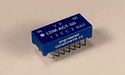
LOGIC DELAY MODULES
LDM-ACT-XX
ACT Logic Delay Module
- T²L compatible input and outputs
- Standby power 5 nano watts max.
- Delays stable and precise
- 16-pin DIP package (.240 high)
- Available in delays from 10 to 250ns
- 5 outputs - each isolated and with 10 T²L fan-out capacity
- Fast rise time on all outputs
DESIGN NOTES
The "DIP Series" Logic Delay Modules developed by Engineered Components Company
have been designed to provide precise tapped delays with required driving and pick-off
circuitry contained in a single 16-pin DIP package compatible with Schottky T²L,
Advanced CMOS and Fast circuits. These logic delay modules are of hybrid
construction utilizing the proven technologies of active integrated circuitry and of passive
networks utilizing capacitive, inductive and resistive elements. The MTBF on these
modules, when calculated per MIL-HDBK-217 for a 50°C ground fixed environment, is in
excess of 1.3 million hours. Module design includes compensation for propagation
delays and incorporates internal termination at the output; no additional external
components are needed to obtain the desired delay.
The LDM-ACT is offered in twenty-six (26) delays from 10ns to 250ns, with each module
incorporating taps as shown in the Part Number Table. Delay tolerances are maintained
as shown in the table, when tested under the "Test Conditions" shown. Delay time is
measured at the +1.5V level on the leading edge. Rise time for all modules is 4ns
maximum when measured from 0.75V to 2.4V. Temperature coefficient of delay is
approximately +500 ppm/°C over the operating temperature range of -40 to +85°C.
These modules accept either logic "1" or logic "0" inputs and reproduce the logic at the
selected output tap without inversion. The delay modules are intended for use with
positive going pulses and are calibrated to the tolerances shown in the table on rising
edge delay; in applications using falling edge timing, it is recommended that a special
unit be calibrated for the specific application. Each module has the capability of driving
up to 20 T²L loads with a maximum of 10 loads on any one tap.
These "DIP Series" modules are packaged in a 16-pin DIP housing, molded of flame-
proof Diallyl Phthalate per ASTM D 5948, Type SDG-F, and are fully encapsulated in
epoxy resin. Leads meet the solderability requirements of MIL-STD-202, Method 208.
Corner standoffs on the housing provide positive standoff from the printed circuit board to
permit solder-fillet formation and flush cleaning of solder-flux residues for improved
reliability.
Marking consists of manufacturer's name, logo (EC²), part number, terminal identification
and date code of manufacture. All marking is applied by silk screen process using white
epoxy paint in accordance with MIL-STD-130, to meet the permanency of identification
required by MIL-STD-202, Method 215.
TEST CONDITIONS
*1. All measurements are made at 25°C.
2. Vcc supply voltage is maintained at 5.0V DC.
3. All units are tested using an ACT toggle-type positive input pulse and one ACT load at
the output being tested.
4. Input pulse width used is 600ns. Pulse period is 5000ns.
OPERATING SPECIFICATIONS
*Delays increase or decrease approximately 2% for an increase or decrease of 5% in
supply voltage.
PART NUMBER TABLE
ø DELAYS AND TOLERANCES (in ns)
ø All modules can be operated with a minumum input pulse width of 40% of full delay
and pulse period approaching square wave; since delay accuracies may be somewhat
degraded, it is suggested that the module be evaulated under the specific operating
conditions.
Special modules can be readily manufactured to improve accuracies and/or provide
customer specified random delay times for specific applications.
Vcc supply voltage: ............ 4.75 to 5.25V DC
Vcc supply current:
Constant "1" or "0" in ...... 1na typical
Constant 1 Mhz square wave .. 4ma typical
Logic 1 input:
Voltage ................ 2V min.; Vcc max.
Logic 0 input:
Voltage ................ 0.8V max.
Logic 1 Voltage out: ........... 4.3V min.
@ -24ma
Logic 0 Voltage out: ........... 0.44V max.
@ +24ma
Operating temperature range: ... -40 to +85°C.
Storage temperature: ........... -55 to +125°C.
Part Number Tap 1 Tap 2 Tap 3 Tap 4
Output
LDM-ACT-1 6 ±1.0 7 ±1.0 8 ±1.0 9 ±1.0 10 ±1.0
LDM-ACT-1 6 ±1.0 8 ±1.0 10 ±1.0 12 ±1.0 14 ±1.0
LDM-ACT-18 6 ±1.0 9 ±1.0 12 ±1.0 15 ±1.0 18 ±1.0
LDM-ACT-22 6 ±1.0 10 ±1.0 14 ±1.0 18 ±1.0 22 ±1.0
LDM-ACT-26 6 ±1.0 11 ±1.0 16 ±1.0 21 ±1.0 26 ±1.0
LDM-ACT-30 6 ±1.0 12 ±1.0 18 ±1.0 24 ±1.0 30 ±1.0
LDM-ACT-35 7 ±1.0 14 ±1.0 21 ±1.0 28 ±1.5 35 ±1.5
LDM-ACT-40 8 ±1.0 16 ±1.0 24 ±1.5 32 ±1.5 40 ±1.5
LDM-ACT-45 9 ±1.0 18 ±1.0 27 ±1.5 36 ±1.5 45 ±2.0
LDM-ACT-50 10 ±1.0 20 ±1.0 30 ±1.5 40 ±2.0 50 ±2.0
LDM-ACT-55 11 ±1.0 22 ±1.0 33 ±1.5 44 ±2.0 55 ±2.0
LDM-ACT-60 12 ±1.0 24 ±1.0 36 ±1.5 48 ±2.0 60 ±2.0
LDM-ACT-65 13 ±1.0 26 ±1.5 39 ±1.5 52 ±2.0 65 ±2.5
LDM-ACT-70 14 ±1.0 28 ±1.5 42 ±2.0 56 ±2.0 70 ±2.5
LDM-ACT-75 15 ±1.0 30 ±1.5 45 ±2.0 60 ±2.5 75 ±2.5
LDM-ACT-80 16 ±1.0 32 ±1.5 48 ±2.0 64 ±2.5 80 ±3.0
LDM-ACT-85 17 ±1.0 34 ±1.5 51 ±2.0 68 ±2.5 85 ±3.0
LDM-ACT-90 18 ±1.0 36 ±1.5 54 ±2.0 72 ±2.5 90 ±3.0
LDM-ACT-95 19 ±1.0 38 ±1.5 57 ±2.0 76 ±2.5 95 ±3.0
LDM-ACT-100 20 ±1.0 40 ±1.5 60 ±2.0 80 ±3.0 100 ±3.0
LDM-ACT-125 25 ±1.0 50 ±2.0 75 ±2.5 100 ±3.0 125 ±4.0
LDM-ACT-150 30 ±1.5 60 ±2.0 90 ±3.0 120 ±4.0 150 ±5.0
LDM-ACT-175 35 ±1.5 70 ±2.5 105 ±4.0 140 ±5.0 175 ±5.0
LDM-ACT-200 40 ±1.5 80 ±2.5 120 ±4.0 160 ±5.0 200 ±6.0
LDM-ACT-225 45 ±2.0 90 ±3.0 135 ±4.0 180 ±6.0 225 ±7.0
LDM-ACT-250 50 ±2.0 100 ±3.0 150 ±4.5 200 ±6.0 250 ±8.0
:: Site Create d by KLM De signs ::
© Copyright 2011, Cornucopia Tool & Plastics, Inc.
All Rights Reserved.
[Top]


